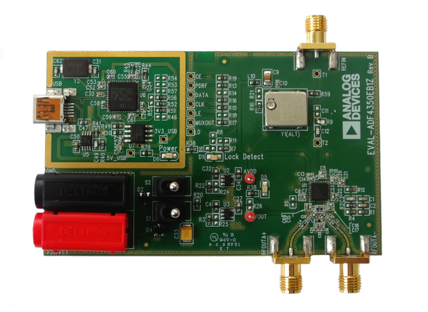
ADF4350

ADF4350: Wideband Synthesizer with Integrated VCO
The circuit shown in Figure 1 uses the ADF4350, a fully integrated fractional-N PLL IC, and the ADL5385 wideband transmit modulator.
The ADF4350 provides the local oscillator (the LO is twice the modulator RF output frequency) signal for the ADL5385 transmit quadrature modulator, which upconverts analog I/Q signals to RF. Taken together, the two devices provide a wideband baseband I/Q-to-RF transmit solution.
The ADF4350 is powered off the ultralow noise 3.3 V ADP150 regulator for optimal LO phase noise performance. The ADL5385 is powered off a 5 V ADP3334 LDO. The ADP150 LDO has an output voltage noise of only 9 μV rms, integrated from 10 Hz to 100 kHz, and helps to optimize VCO phase noise and reduce the impact of VCO pushing (equivalent to power supply rejection). See CN-0147 for more details on powering the ADF4350 with the ADP150 LDO.
The ADL5385 uses a divide-by-2 block to generate the quadrature LO signals. The quadrature accuracy is, thus, dependent on the duty cycle accuracy of the incoming LO signal (as well as the matching of the internal divider flip-flops). Any imbalance in the rise and fall times causes even order harmonics to appear, as evident on the ADF4350 RF outputs. When driving the modulator LO inputs differentially, even-order cancellation of harmonics is achieved, improving the overall quadrature generation. (See “Wideband A/D Converter Front-End Design Considerations: When to Use a Double Transformer Configuration.” Rob Reeder and Ramya Ramachandran. Analog Dialogue, 40-07.)
Because sideband suppression performance is dependent on the modulator quadrature accuracy, better sideband suppression is achievable when driving the LO input ports differentially vs. single-ended. The ADF4350 has differential RF outputs compared to a single-ended output available on most competitor PLL devices with integrated VCO.
The ADF4350 output match consists of the ZBIAS pull-up and, to a lesser extent, the decoupling capacitors on the supply node. To get a broadband match, it is recommended to use either a resistive load (ZBIAS= 50 Ω) or a resistive in parallel with a reactive load for ZBIAS. The latter gives slightly higher output power, depending on the inductor chosen. An inductor value of 19 nH or greater should be used for LO operation below 1 GHz. The measured results in this circuit were performed using ZBIAS = 50 Ω and an output power setting of +5 dBm. When using the 50 Ω resistor, this setting gives approximately 0 dBm on each output across the full band, or +3 dBm differentially. The ADL5385 LO input drive level specification is −10 dBm to +5 dBm; therefore, it should be possible to reduce the ADF4350 output power to save current.
A sweep of sideband suppression versus RF output frequency is shown in Figure 2. In this sweep, the test conditions were as follows: baseband I/Q amplitude = 1.4 V p-p differential sine waves in quadrature with a 500 mV dc bias; baseband I/Q frequency (fBB) = 1 MHz; LO = 2 × RFOUT. A simplified diagram of the test setup is shown in Figure 3. A modified ADL5385 evaluation board was used because the standard ADL5385 board does not allow a differential LO input drive.
This circuit achieves comparable or improved sideband suppression performance when compared to driving the ADL5385 with a low noise RF signal generator, as used in the data sheet measurement. Using the differential RF outputs of the ADF4350 provides even-order harmonic cancellation and improves modulator quadrature accuracy. This impacts sideband suppression performance and EVM (error vector magnitude). A single carrier W-CDMA composite EVM of better than 2% was measured with the circuit shown in Figure 1. The solution thus provides a low EVM broadband solution for frequencies from 68.75 MHz to 2.2 GHz. For frequencies above 2.2 GHz, a divide-by-1 modulator block should be used, as described in CN-0134.
A complete design support package for this circuit note can be found at http://www.analog.com/CN0144-DesignSupport.
